News
X-FAB introduces image sensor back illumination technology to enhance CMOS sensor performance
- Source:Network finishing
- Release on:2024-04-09
Beijing, China, April 9, 2024-The global recognized and excellent simulation/hybrid signal wafer factory factory X-Fab Silicon Foundries ("X-Fab") announced today that its optical sensor product platform adds new members- In order to meet the requirements of the performance of the new generation of image sensor, X-Fab has now opened the back photo (BSI) function on its popular CMOS sensor craft platform XS018 (180 nanote).

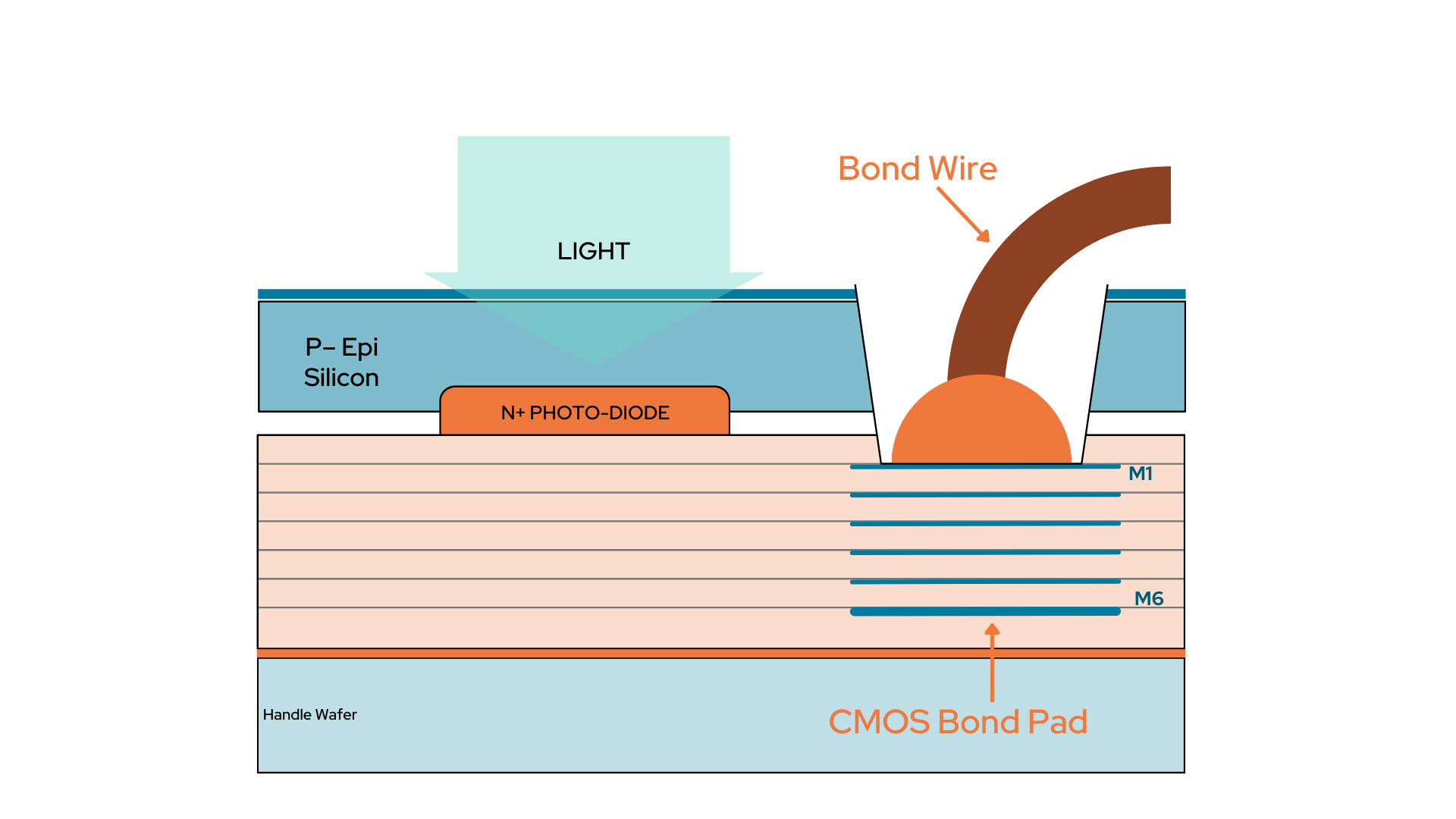
BSI craft section schematic diagram
Through the BSI process, the imaging sensor pixel performance will be greatly enhanced.This technology allows each pixel to receive the incident light from the metal layer of the back -end process, which greatly enhances the filling ratio of the sensor, up to 100%.Because it can obtain higher pixel sensitivity, this advantage is particularly significant under dark light conditions.At the same time, due to the shortening of the optical path, the BSI process can effectively reduce the string between adjacent pixels, and then improve the image quality of the image.Although BSI technology is currently widely used in 300 mm wafers and is widely used on consumer -grade pixel image sensors, for the 200mm wafer market, it is mainly used in industrial medical vehicles and other fields; or for stitching through stitching through stitching The large pixel image sensor, especially in the scenario that requires additional customization, has a very limited choice of BSI technology on the market.Therefore, X-FAB has added the BSI function in XS018, the original CMOS sensor process platform, which has been well received, bringing new possibilities to different market segments. Whether it is X-ray diagnostic equipment, industrial automation system, astronomical research, or robot Navigation, car front camera, etc., customers can easily meet the most stringent application needs.

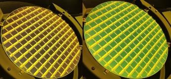
The BSI process and standards can be visible to the light wave segment anti -reflective layer (left). The wafer uses the BSI process and the near -infrared band anti -reflective layer (right)
The XS018 CMOS sensor platform has the characteristics of fast reading speed and low dark current. Customers can also select a variety of different extension layers on this platform to achieve image sensors for different application scenarios.In addition, through the BSI process, customers can also choose to add ARC layers and adjust them according to different special application requirements.The attached X-FAB design supports the complete workflow of the initial design to engineering sample transportation, which also includes a complete PDK.
"BSI technology can place the light sensing element closer to the light source and avoid unnecessary circuit obstruction to improve image imaging capabilities. Therefore, it has been used in modern imaging devices. It is useful. "Heming Wei, a technical marketing manager of X-FAB optical sensor, said." Although such applications were mainly concentrated in the consumer electronics field, there are currently a large number of demands in the industrial, automotive and medical markets. With the help of X-Fab's BSI technology, It can gather the advantages of higher sensitivity, larger sensor size, and pixel capacity, and launch market convincing products to meet different application needs of industry, automobiles, and medical treatment to a greater extent. "
Sumid language:
ARC anti -reflection coating
BSI back photo technology
CMOS complementary metal oxide semiconductor
PDK craft design kit
###
About X-FAB:
X-FAB is the leading simulation/hybrid signal and MEMS wafer foundry group to produce silicon wafers for automotive, industry, consumption, medical care and other applications.The X-FAB uses a modular CMOS and SOI process from 1.0 μm to 110nm, and its long life process of SIC and Microelectronics System (MEMS) to create the highest quality standards, excellent manufacturing technology and innovation for global customers. solution.X-Fab's simulated digital integration circuit (hybrid signal IC) and sensor MEMS are produced in six production bases in Germany, France, Malaysia and the United States, and have about 4,200 employees worldwide.www.xfab.com